
The Global Advanced Semiconductor Packaging is analyzed in this report across packaging type, device type, end-use, and region, highlighting major trends and growth forecasts for each segment
Introduction:
Advanced semiconductor packaging encompasses a set of manufacturing techniques that integrate multiple semiconductor chips into a single, high-performance electronic package. As traditional scaling approaches face physical and economic constraints, advanced packaging has emerged as a pivotal enabler of innovation, unlocking new frontiers in performance, efficiency, and miniaturization across a range of industries.
The global advanced semiconductor packaging market is gaining substantial momentum, projected to reach USD 50.2 billion by 2030. In 2024, the market stood at approximately USD 36.8 billion and is expected to grow at a CAGR of 7.5% during the forecast period. This growth is underpinned by the accelerating adoption of 5G, AI, IoT, and high-performance computing. As demand intensifies for smarter devices and edge processing capabilities, semiconductor packaging has evolved from a post-design consideration into a strategic lever for innovation and competitive differentiation.
Market Dynamics:
The advanced semiconductor packaging market is undergoing significant evolution, driven by increasing demand for high-performance, energy-efficient chips across a broad set of applications—including 5G, AI, HPC, and automotive systems. With Moore’s Law decelerating, the industry is turning to advanced packaging formats such as 2.5D/3D ICs, fan-out wafer-level packaging (FOWLP), and system-in-package (SiP) to push the performance envelope without scaling chip dimensions. These technologies enable higher functional density, improved thermal performance, and faster interconnects, making them indispensable to the next generation of compute architectures.
A major contributor to market acceleration is the automotive sector. Global vehicle production rose to approximately 85 million units in 2022, up from 80 million the previous year. Each vehicle incorporates hundreds of semiconductor components—spanning ADAS, infotainment, and power systems—substantially boosting demand for sophisticated packaging solutions.
The adoption of heterogeneous integration and chiplet architectures is also reshaping the ecosystem. These designs allow manufacturers to combine diverse IP blocks and process nodes within a single package, offering unmatched design flexibility. As workloads become more compute-intensive, industries from consumer electronics to aerospace are increasingly relying on these packaging techniques to deliver compact, high-performance systems.
Further tailwinds come from rising investments in AI servers, EVs, and IoT infrastructure. Government-led initiatives such as India’s ‘Digital India’ and ‘Make in India’ programs, along with liberalized FDI policies, are attracting significant foreign investment into semiconductor packaging. These efforts are enhancing domestic manufacturing capabilities and reinforcing India’s strategic role in the global semiconductor supply chain.
The market is also seeing strong demand from AI and data center expansion, where high-bandwidth memory (HBM) and advanced interposer technologies are essential. Meanwhile, the rise of edge computing and wearables is prompting a shift toward smaller, power-optimized packaging formats. OSATs and foundries are investing heavily in new packaging lines and R&D initiatives to capture share in this rapidly evolving space.
Emerging trends include hybrid bonding for 3D stacking, the convergence of photonics and semiconductor packaging, and the development of chiplet ecosystems backed by standardized interfaces such as UCIe. Sustainability is also rising on the agenda, with manufacturers exploring low-emission materials and greener processes. As device complexity increases, advanced packaging is no longer a technical enhancement—it is a critical differentiator across the semiconductor value chain.
Segment Highlights and Performance Overview:
By Packaging Type
Flip Chip Packaging (FCP) leads the market by packaging type, accounting for approximately 38% to 40% of global share. Its widespread use is attributed to its superior I/O density, thermal management, and electrical performance, making it ideal for logic-heavy and high-speed applications. Growing demand across consumer electronics, automotive systems, and networking equipment continues to reinforce FCP’s market dominance.
By Device Type
Logic Devices represent the largest share in the device type segment, contributing over 28% to the market. This category includes CPUs, GPUs, and SoCs—all of which require advanced packaging formats such as 2.5D/3D ICs and fan-out designs to support escalating bandwidth and processing needs. The proliferation of AI, data center computing, and edge devices is further driving packaging innovation around logic components.
By End Use
Consumer Electronics is the dominant end-use category, comprising roughly 51% to 52% of the total market. The continued expansion of smartphones, laptops, wearables, and smart home products is fueling demand for compact, high-performance packages. As AI, AR/VR, and IoT features become standard in consumer devices, advanced packaging is playing a critical role in enabling miniaturization and multifunctionality.
Geographical Analysis:
The global advanced semiconductor packaging market is segmented across North America, Europe, Asia-Pacific, South & Central America, and the Middle East & Africa.
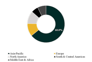
Asia-Pacific commands the largest share, generating approximately 60% of total global revenue. This leadership is anchored by mature semiconductor manufacturing hubs in China, Taiwan, South Korea, and Japan, supported by a well-developed OSAT and foundry infrastructure.
North America, meanwhile, is projected to record the highest CAGR, estimated at approximately 11.1%. This growth is being driven by strategic investments in AI, high-performance computing, and 5G infrastructure, alongside strong policy support from government initiatives like the CHIPS and Science Act. These measures are enhancing domestic capabilities in both semiconductor fabrication and advanced packaging.
Competition Landscape:
The competitive landscape in the advanced semiconductor packaging market is shaped by the presence of leading integrated device manufacturers (IDMs), foundries, OSAT providers, and materials suppliers. Players are focusing on R&D, capacity expansion, and cross-industry collaborations to secure a foothold in fast-growing verticals such as AI, automotive, and 5G.
Key companies profiled in this report include:
Intel Corporation, Samsung Electronics Co., Ltd., Micron Technology, Inc., Texas Instruments Incorporated, SK hynix Inc., ASE Technology Holding Co., Ltd., Amkor Technology, Inc., JCET Group Co., Ltd., Powertech Technology Inc., and UTAC Holdings Ltd.
These firms are pushing the frontier of advanced packaging through heterogeneous integration, chiplet strategies, and next-gen interconnect solutions—strengthening their positions in a rapidly consolidating market.
Recent Developments:
Segmentations
Packaging Type:
Device Type:
By End Use:
Companies: